


-
CN0518 User Guide5/18/2023WIKI
CN0518
USB-Powered, 915 MHz RF Low Noise Amplifier Receiver with Overpower Protection Circuit
Top
Overview
Design Resources
Design & Integration Files
- Schematic
- Bill of Materials
- Gerber Files
- Assembly Files
- Allegro Layout
Evaluation Hardware
Part Numbers with "Z" indicate RoHS Compliance. Boards checked are needed to evaluate this circuit.
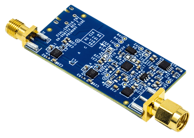
- EVAL-CN0518-EBZ ($41.20) 900 MHz ISM Band Low Noise Receive Amplifier
Device Drivers
Software such as C code and/or FPGA code, used to communicate with component's digital interface.
Features & Benefits
- +25 dB of Rx Signal Gain
- 50 ohm Input and Output Impedance
- Overvoltage Input Protection
- SMA Input and Output Connectors
- USB Powered
Documentation & Resources
Circuit Function & Benefits
The International Telecommunication Union allocates the unlicensed 915 MHz, industrial, scientific and medical (ISM) radio frequency band for use in Region 2, geographically consisting of the Americas, Greenland, and some Eastern Pacific Islands. Advancements in wireless technologies and standards within the region have made the band popular for short range, wireless communication systems.
The 915 MHz ISM band places no restrictions on the application or duty cycle and common uses include amateur radio, supervisory control and data acquisition (SCADA), and radio frequency identification (RFID) systems.
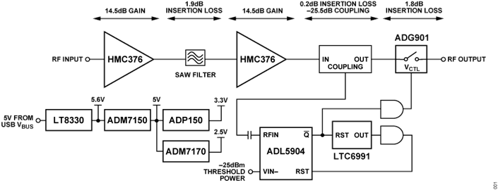
The circuit shown in Figure 1 is a two-stage RF low noise amplifier (LNA) optimized for receiver signal chains in the 915 MHz ISM band. At the center frequency, the circuit results in a forward gain (S21) of 25 dB and an input return loss (S11) of more than 10 dB. The RF input and output ports are designed with a 50 Ω impedance match, enabling a direct connection between the circuit and a standard 50 Ω system.
The board includes a high speed overpower cutoff that protects sensitive downstream equipment connected to the receiver system. The receiver system also automatically returns to normal operation when the RF power level drops within the acceptable range. The RF inputs and outputs are standard subminiature version A (SMA) connectors, and the entire design is powered by a single micro- USB connector.


Circuit Description
RF LOW NOISE AMPLIFIER
The CN0518 uses cascaded HMC376 low noise amplifiers for its RF signal path, achieving an overall gain of approximately 25 dB. The HMC376 is a gallium arsenide (GaAs), pseudomorphic high electron mobility transistor (pHEMT), high MMIC, low noise amplifier that operates from 700 MHz to 1000 MHz.
Figure 2 shows the typical S-Parameter performance, with a typical gain of 15 dB and return losses of more than 10 dB throughout the entire frequency range. The HMC376 has a typical noise figure of 0.7 dB, a 1 dB compression point (P1dB) of 21.5 dBm, and a third-order intercept point (OIP3) of 36 dBm.


Impedance Matching Network
The HMC376 RF input and output ports are internally matched for a single-ended 50 Ω impedance. This internally matched topology allows the HMC376 to be readily ported between any printed circuit board material regardless of its dielectric constant, thickness, or composition. The RFOUT also has an integrated DC-blocking capacitor that eliminates the need for an external capacitor. The only requirement needed is an inductor in parallel with the RF input with respect to the ground.
Figure 3 shows the basic configuration and implementation of two cascaded HMC376 amplifiers.


RF SAW FILTER
The first stage amplifier output of the CN0518 is filtered by a surface wave acoustic (SAW) filter, which eliminates unwanted out-of-band amplification. When selecting a filter, a balance must be struck between the band flatness and the out-of-band rejection. SAW filters are also a source of insertion loss, which reduces the overall gain of the signal chain and needs to be considered during selection.
The filter used has a pass band of 902 MHz to 928 MHz, with a return loss of 21 dB and an insertion loss of 1.9 dB at 915 MHz center frequency.
RF DIRECTIONAL COUPLER
The CN0518 includes a multilayer RF directional coupler. This device has an operating frequency of 698 MHz to 2.62 GHz with a coupling factor of 25.5 at 915 MHz. It has an input and output port impedance of 50 Ω and a typical insertion loss of 0.2 dB.
RF SWITCH
The ADG901 is a wideband RF switch that uses a CMOS process to provide high isolation and low insertion loss. It is an absorptive (matched) switch with 50 Ω terminated shunt legs. The switch enables the user to pass DC signals up to 0.5 V without the use of a DC-blocking capacitor.
The ADG901 operates at DC up to 4.5 GHz at -3 dB frequency. At the 915 MHz center frequency, this device has a typical insertion loss of approximately 1.8 dB at "ON state" as shown in Figure 4, and a typical isolation loss of approximately 30 dB at "OFF state" as shown in Figure 5.


Combining the insertion loss from the filter, coupler, and the RF switch results in a total insertion loss of approximately 3.9 dB at the output of the RF switch in normal operating conditions.
RF PERFORMANCE
The resulting S-parameters, phase noise measurements, spurious-free dynamic range (SFDR), noise figure, and stability measure of the CN0518 are shown in the figures below.
At the center frequency of 915 MHz, the CN0518 achieves a gain of 25 dB with input and output return losses of greater than 10 dB. Figure 6 shows the S-Parameters across the operating frequency range.


Figure 7 shows the single sideband phase noise at 915 MHz, with approximately -91 dBc/Hz, -125 dBc/Hz, -129 dBc/Hz, and -142 dBc/Hz at frequency offsets of 10 Hz, 1 kHz, 100 kHz, and 1 MHz offset, respectively.


Figure 8 shows the narrow-band single-tone RF output with an SFDR of 76 dBFS.


Figure 9 shows the corresponding noise figure of approximately 0.8 dB over the entire frequency range.


The system is stable across the entire 915 MHz ISM frequency bandwidth with the Rollet's stability factor (k) being above 1 and the supplementary stability measure (B1) being above 0, as shown in Figure 10. This makes the CN0518 unconditionally stable for any source and load impedance combination.


OVERPOWER PROTECTION
An overpower management feature is implemented in CN0518 wherein the RF path of the board is automatically isolated when the output power reaches the preset threshold. This feature is performed using an ADL5904 RF power detector.
The ADL5904 provides a resistor-programmable detection threshold, which compares the voltage from an internal envelope detector with a user-defined input voltage. When the voltage from the envelope detector exceeds the user-defined threshold voltage at the VIN- pin, an internal comparator captures and latches the event to a set/reset (SR) flip-flop. Figure 11 shows the overpower protection circuitry for the CN0518.


As shown in Figure 11, the amplified RF input is sampled by a 25.5 dB RF directional coupler. This power is forwarded to the RFIN pin of the ADL5904, which is then sampled by the internal envelope detector. The ADL5904 threshold voltage level on VIN- pin is set by a resistor divider network, which value can be computed using Equation 1:

where:
VIN- is the voltage level at the VIN- pin of the ADL5904.
R1 is the user-defined resistance value.
R2 is the user-defined resistance value.
IBIAS is the input bias current.
The CN0518 was set at -25 dBm input threshold power, which is equivalent to 0 dBm RF output to protect any sensitive downstream equipment connected to the receiver system. Table 1 can be found in the ADL5904 data sheet and shows the -25 dBm threshold power corresponds to a VIN- voltage level of 17 mV when operating at 900 MHz.
| Input Threshold Power (dBm) |
Threshold Voltage (mV) |
||
| 100 MHz | 900 MHz | 1900 MHz | |
| -25 | 18 | 17 | 16 |
| -24 | 20 | 18 | 17 |
| -23 | 22 | 20 | 19 |
| -22 | 24 | 22 | 21 |
| -21 | 26 | 25 | 23 |
The threshold level on VIN- is set by a resistor divider. The value of R1 is primarily chosen to minimize loading on the 3.3 V rail, and R2 is chosen for an output impedance that is insensitive to leakage and bias currents. Setting R1 to 10 kΩ and using the power threshold value of 17 mV, the R2 value is calculated using Equation 1:
VIN- = 17 mV
IBIAS = 20 μA
R1 = 10 kΩ
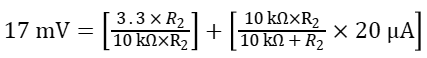
R2 = 48.8 Ω or 49.9 Ω (using standard resistor value)
Solving Equation 1 using the closest standard resistor value sets the VIN- voltage level at 17 mV. This user-defined VIN- voltage is then compared to the output voltage of the internal envelope detector, which is driven by the RF input level. When the power exceeds the threshold value, an overpowering event occurs which opens or isolates the RF path. The series combination of R1 and R2 results in a negligible divider current of 328 μA.
The ADL5904 introduces an error level of up to +2.5 dBm on its RF threshold power and can vary from device-to-device. If an accurate threshold power is required, a simple calibration routine must be performed to compensate for the device-to-device variation. Refer to the ADL5904 data sheet for more information on the calibration routine.
Automatic Reset Feature
The CN0518 also includes an automatic reset circuitry that activates when the power level returns within the acceptable range. This feature is done through the LTC6991, a programmable low frequency timer.
As shown in Figure 12, the Q output of the ADL5904 holds the LTC6991 in reset mode during normal operation. When an overpowering event occurs, the LTC6991 is enabled and a 4 ms delay begins. The ADL5904 resets after 4 ms, effectively resampling the power level. If the overpowering condition persists, the ADL5904 trips again and the control signal of the RF switch enters the low state. This shift in signal isolates the RF input and output of the ADG901 switch. Once the overpower event subsides, the ADL5904 starts to resample the power level and then returns to its normal operation.


Overpower Protection Test
Figure 13 presents the setup used to test the overpower protection functionality of the CN0518. In this test, the RF signal generator is set to 915 MHz center frequency and the power to the input is ramped up from -25 dBm to -15 dBm. The CN0518 output power is monitored using a high speed oscilloscope, which shows the response time from the overpowering event to the output power being attenuated.
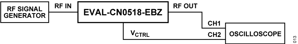
Figure 14 shows the overpowering protection response time. Based on the figure, the output of the CN0518 has a response time of approximately 10 ns from its normal operation to the RF output power being attenuated.


Figure 15 shows the recovery time from when the overpowering condition subsides, and the power level returns back to its acceptable range. The data demonstrate a 5 ns delay from the attenuated RF output to its normal operation.


USB POWER MANAGEMENT
The CN0518 sources its power through a micro-USB adapter, which typically provides a 5 V, 1 A supply via the micro-USB port. The nominal 4.75 V to 5.25 V input from the USB port is boosted to 5.6 V, then post-regulated to 5.0 V, 3.3 V, and 2.5 V. The circuit requires an overall current of approximately 260 mA from the USB supply during normal operation.
Figure 16 shows the complete CN0518 power tree.


SEPIC Converter
The LT8330 is a current-mode DC/DC converter capable of generating either positive or negative output voltages. It can be configured as boost, SEPIC, or inverting converter consuming as low as 6 μA of quiescent current. Figure 17 shows the basic configuration needed to set the LT8330 for a 5.6 V output.


The output voltage is programmed with resistor divider from the output to the FBX pin of the LT8330. Equation 2 shows how to calculate a desired output voltage with the user-defined resistor values:

where:
VOUT is the desired output voltage in Volts.
R1, R2 are the user-defined resistor values.
For the required output voltage of 5.6 V, the equation results with R1 = 590 kΩ and R2 = 232 kΩ.
Ultralow Noise Linear Regulator
The 5 V output from the ADM7150 is used to power the two HMC376 LNAs. The ADM7150 is a low dropout linear regulator with a typical noise of 1 μV rms from 100 Hz to 100 kHz for fixed output voltage options and <1.7 nV/√Hz noise spectral density above 10 kHz.
The ADP150 is used to generate 3.3 V for powering the RF detector and auto retry circuit. It is a high performance low dropout linear regulator featuring an ultralow noise and ultra high PSSR architecture for powering noise sensitive RF applications.
An ADM7170-2.5 LDO regulator is used to generate the supply voltage required by the ADG901 RF switch. This device has an input voltage range of 2.3 V to 6.5 V and a fixed output voltage of 2.5 V. The ADM7170-2.5 only requires capacitors for proper operation. Particularly, the ADM7170-2.5 is compatible to use small decoupling capacitors of 4.7 μF on its input and output pins.
Common Variations
The ADL5523 can be used as an alternative low noise amplifier for applications using the 915 MHz ISM band. This device offers a slightly higher gain (S21) and a low noise figure at a cost of having lower return losses (S11, S22), output third-order intercept, and 1 dB compression point.
The ADG902 can also be used as the RF switch, this device is pin-compatible and shares the same specifications as the ADG901, but it is a reflective switch and offers lower isolation loss.
Analog Devices, Inc. also offers a similar reference design for receiver amplifiers operating in the 433.92 MHz, 2.4 GHz, and 5.8 GHz ISM bands. For more information, please refer to the CN0555, CN0521, and CN0534 circuit notes.
If you are working in the 915 MHz ISM band and needs a transmit signal chain solution, refer to the CN0522 reference design.
Circuit Evaluation & Test
This section describes the setup and procedure for the CN0518 circuit evaluation. For complete details, refer to the CN0518 User Guide.
EQUIPMENT NEEDED
- EVAL-CN0518-EBZ circuit evaluation board
- Signal generator (Rohde & Schwarz® SMA100B)
- Signal analyzer (Keysight® E5052B)
- Vector network analyzer (Keysight N5242A PNA-X)
- 5 V, ≥0.5 A AC/DC power adapter with micro-USB cable
- SMA cables
SETUP AND TEST
Figure 18 shows the functional block diagram for the S-Parameter and noise figure test setup.


The procedure for measuring S-Parameters and the noise figure are as follows:
- Set the measurement conditions of the vector network analyzer as follows:
- Set the frequency span from 902 MHz to 928 MHz.
- Set the frequency step size to 10 kHz.
- The power level must be less than or equal to -30 dBm.
- Perform a full 2-port calibration of the vector network analyzer using a calibration kit. Note that the RF output of the EVALCN0518-EBZ can be connected directly to a test port, so that only one measurement cable is needed for the test setup.
- Connect the EVAL-CN0518-EBZ across the test ports of the vector network analyzer using the calibrated test setup.
- Power up the EVAL-CN0518-EBZ using the 5 V power adapter.
- Set the vector network analyzer to display the traces of the individual S-Parameters and the noise figure.
- Compare the measurements to the expected values. At 915 MHz center frequency, the values for input and output return losses are approximately -20 dB and -12 dB, respectively. For the gain and noise figure readings, values should be approximately 25 dB and 0.8 dB, respectively.
Figure 19 shows the functional block diagram for the phase noise and SFDR test setup.


To perform the phase noise and SFDR tests, follow the steps below:
- Set the measurement configuration of the signal analyzer as follows:
- For SFDR measurement, set the center frequency to 915 MHz, the frequency span to 902 MHz to 928 MHz, and the RF amplitude to -30 dBm.
- For phase noise measurement, set the center frequency to 915 MHz and the offset frequency range to 10 Hz to 30 MHz.
- Set the power level of the signal generator between -30 dBm to -20 dBm with a center frequency set at 915 MHz.
- Connect the signal generator output to the RF input of the EVAL-CN0518-EBZ.
- Connect the RF output of the EVAL-CN0518-EBZ to the signal analyzer.
- Power up the EVAL-CN0518-EBZ using the 5 V power adapter.
- Execute a measurement run on the signal analyzer.
- Using the signal analyzer, get the phase noise value and verify if it is approximately -129 dBc/Hz at 100 kHz offset.
- Run the SFDR test and compare the readings; expected value is approximately 76 dBFS.
Discussions
Sample Products
Evaluation Boards
Pricing displayed is based on 1-piece.
Up to two boards can be purchased through Analog.com. To order more than two, please purchase through one of our listed distributors.
Pricing displayed is based on 1-piece. The USA list pricing shown is for budgetary use only, shown in United States dollars (FOB USA per unit), and is subject to change. International prices may vary due to local duties, taxes, fees and exchange rates.