


-
CN0550 User Guide6/23/2023WIKI
Overview
Design Resources
Design & Integration Files
- Schematic
- Bill of Materials
- Gerber Files
- Assembly Drawing
- Allegro Layout File
Evaluation Hardware
Part Numbers with "Z" indicate RoHS Compliance. Boards checked are needed to evaluate this circuit.
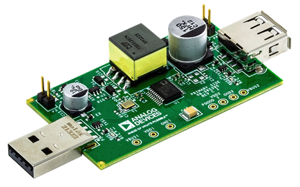
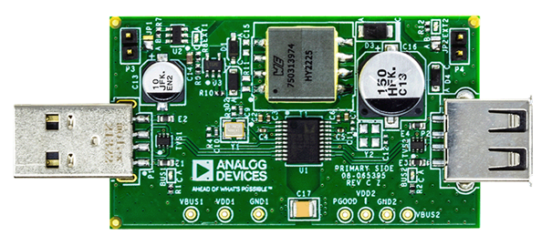
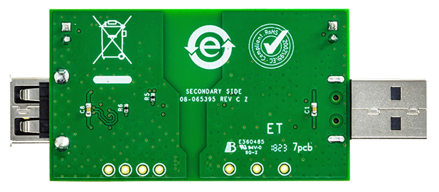
- EVAL-CN0550-EBZ ($40.00) High Speed Isolated USB 2.0 Board
Features & Benefits
- Isolated Low-speed, Full-speed, and High-speed USB 2.0
- Auto Negotiation of USB Interface Speed
- Delivers Isolated Power from the Host
- Isolation Rating up to 1.75kV RMS
- Standard USB Type A Connectors onboard
Markets and Technologies
Parts Used
Documentation & Resources
Circuit Function & Benefits
Since its introduction in 1996, USB has become the standard, point-to-point, serial communication interface for handheld devices, test and measurement equipment, embedded development platforms, and countless other applications. USB has largely replaced RS-232 (serial) and parallel ports.
The USB interface emphasizes simple and robust connections between a host and its peripheral devices, with most of the complexity being abstracted by the USB controller and physical layer. USB devices are self-configuring, widely supported by common operating systems, and plug-and-play. They also offer power delivery, are hot-swappable, and use standardized low-cost, high-insertion life connectors and cables.
USB devices in these environments however, may require the addition of electrical isolation between the host and the peripheral equipment. Isolation requirements can vary depending on the application; medical equipment for example, requires devices capable of withstanding a 5 kV surge voltage to ensure patient safety. For industrial settings, isolation considerations may include susceptibility to electrostatic discharge, lightning strikes and power surges, as well as sensitivity to electrical noise from electromagnetic interference and ground loops.
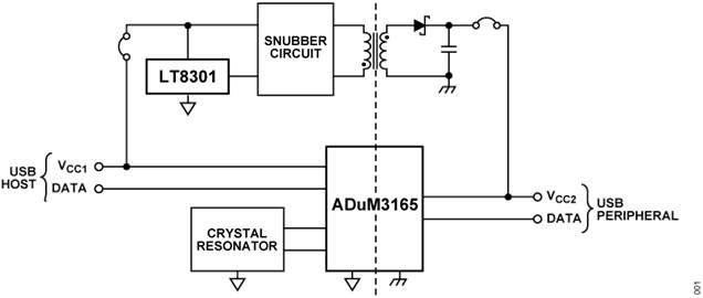
The reference design shown in Figure 1 is a USB 2.0 galvanic isolator that can withstand 1.5 kVAC for one minute and can provide basic insulation for systems with a 50 V rms working voltage. The USB isolator supports a maximum data transfer rate of 480 Mbps, and automatically negotiates the transfer rate based on the capabilities of the connected devices.
The circuit can also supply isolated power to the USB peripheral via a flyback converter. For typical applications, the 5 V bus of the USB host can be used as the input power, which allows a maximum isolated load current of 440 mA to be delivered to the peripheral.


Circuit Description
USB DIGITAL ISOLATION
The CN0550 employs an ADuM3165 digital isolator to provide galvanic isolation of the USB data lines between the host and the peripheral device. The ADuM3165 supports low-speed (1.5 Mbps), full-speed (12 Mbps), and high-speed (480 Mbps) USB 2.0, while maintaining an isolation voltage rating of 3.75 kV rms.
The ADuM3165 utilizes the Analog Devices' iCoupler® technology to implement the isolation on the digital lines, and is capable of automatically negotiating the appropriate data transfer speed without user intervention or the need for external circuitry.


Figure 2 shows the ADuM3165 circuitry, which greatly simplifies the isolation design as the device is highly integrated. Excluding the signals from the USB connectors, the only external circuitry required to operate the device is a 24 MHz reference clock source for the internal phase-locked loop (PLL). This can be implemented either by connecting a crystal between its XI and XO pins, or by connecting a 24 MHz clock source from the host controller to the XI pin and leaving XO floating. In CN0550, a 24 MHz crystal with its necessary load capacitance is connected across the XI and XO pins.
Power to the ADuM3165 is supplied as +5 V on the VBUS1 and VBUS2 pins. VBUS1 is tied directly to the USB host connector, and VBUS2 is tied to the isolated 5 V supply. Internal low dropout (LDO) regulators generate the required +3.3 V VDD1 and VDD2 supplies for internal circuitry. The power dissipation of the LDOs reduces the maximum ambient operating temperature slightly. Refer to the ADuM3165 data sheet for details.
To verify high-speed USB electrical requirement compliance, two signal quality tests were performed using the CN0550. Figure 3 and Figure 4 show open eye diagrams at the far-end and near-end, respectively.


ISOLATED USB POWER
An LT8301 micropower no-opto isolated flyback converter provides the isolated 5 V bus power on the peripheral side. Depending on the input voltage, this device is capable of delivering up to 6 W of isolated output power, allowing it to support both low-power and high-power USB 2.0 devices. Figure 5 shows the simplified isolated flyback circuit configuration used for the CN0550.


In CN0550, the LT8301 uses a flyback transformer with a turns ratio of 3:1 and a primary inductance of 40 μH to produce the isolated power. A diode-Zener snubber is included across the primary winding to protect the device from high voltage spikes generated by leakage inductance. A diode provides rectification on the secondary side, and is rated for a forward current of 5 A and a reverse voltage of 30 V. A 150 μF capacitor is used to reduce the ripple of the output voltage. This combination of components allows the design to meet the standard 100 mA maximum load current drawn by low-power USB 2.0 devices using the available 5 V bus power on the host side.
Additionally, this circuit is capable of supporting the 500 mA maximum load current drawn by high-power USB 2.0 devices when connected to an external power supply of at least 8 V. Higher load currents can be achieved with more input voltage, up to 1.3 A at the maximum input voltage of 32 V. For the general design procedure in selecting these components, refer to the LT8301 data sheet.
Note that while the ADuM3165 has an insulation voltage rating of 3.75 kV rms and the LT8301 has a maximum input voltage of 42 V, these parameters will be limited by the transformer specifications in this application. The flyback transformer used in the CN0550 is tested at 1.5 kV rms insulation, but is only designed to comply with IEC61558-2-16 basic insulation for a primary circuit at a working voltage of 50 V rms. This transformer is suitable for isolation in most laboratory test and measurement applications.
The output voltage of the LT8301 is set by an external feedback resistor connected between the SW and RFB pins; the value of which is calculated using Equation 1:
where:
RFB is the required feedback resistance in Ω.
NPS is the transformer effective primary-to-secondary turns ratio.
VOUT is the output voltage.
VF is the output diode forward voltage.
For the required output voltage of 5 V, a 3:1 transformer turns ratio, and an output diode forward voltage of 0.3 V, Equation 1 results in an RFB value of 159 kΩ; the closest standard 1% value to this is 158 kΩ is considered. In practice, however, the unique sampling scheme used by the LT8301 can introduce errors in the output voltage. Equation 2 can be used to adjust the feedback resistance based on the actual output voltage.
where:
RFB(FINAL) is the adjusted feedback resistance in Ω.
VOUT(MEAS) is the actual output voltage measured in V.
With a target VOUT of 5.0 V, a measured VOUT of 5.26 V and an initial RFB of 158 kΩ, Equation 2 results in a resistance value of 150.19 kΩ. In CN0550, a 150 kΩ ±1% feedback resistor is used. The resulting load regulation using these values are shown in Figure 6.


Common Variations
Certain applications may require devices to be synchronized to a single timing source. In these cases, directly apply a precision 24 MHz clock signal from the system microprocessor to the external clock input of the ADuM3165 instead of using an external crystal. If the system microprocessor and the clock signal is located on the peripheral side rather than the host side, the ADuM3166 may be used as an alternative. This device has the same specifications and pinout as the ADuM3165, with the placement of the XI and XO pins as the only difference.
The ADuM3165 VBUS1, VBUS2 operating voltage range is 3.0 V to 5.5 V, overlapping the VDD1, 2 operating range of 3.0 V to 3.6 V. If a 3.0 V to 3.6 V supply is available on either side, the VDDx pin can be tied to its corresponding VBUSx and powered directly. This also reduces the overall device dissipation and extends the operating temperature range. Refer to the ADuM3165 data sheet for more details.
The isolation voltage rating of the CN0550 is limited by the transformer used in the flyback converter circuit, a different isolated power supply could be used in applications requiring full 3.75 kV rms insulation voltage rating of the ADuM3165.
If even higher insulation ratings are required by the application, the ADuM4165 or the ADuM4166 can be used as an alternative USB digital isolator. Analogous to the ADuM3165 and ADuM3166, these two devices share the same specifications and are pin-compatible except for the placement of the XI and XO pins. The ADuM4165 and ADuM4166 feature a reinforced surge isolation voltage rating of 8 kVPK and a high dielectric insulation voltage rating of 5 kV rms, but also have a larger footprint compared to the ADuM3165 and ADuM3166.
Alternative power solutions, such as the ADuM6020 isolated DC/DC converter, have an insulation voltage rating of 5 kV rms, but is only capable of supplying a maximum current of 100 mA.
The CN0419 circuit note is a smaller, lower power USB digital isolator reference design for applications that do not require high-speed USB 2.0.
Circuit Evaluation & Test
This section covers the setup and procedure for evaluating the CN0550 circuit evaluation board. For complete details, refer to the EVAL-CN0550-EBZ User Guide.
EQUIPMENT NEEDED
- EVAL-CN0550-EBZ
- Host PC (Windows/Linux/Mac)
- A high-speed USB peripheral device (for example, USB flash drive)
SETUP AND TEST
To test the USB 2.0 functionality of the EVAL-CN0550-EBZ, follow the below procedure:
- Connect the peripheral device to the USB port on the EVALCN0550-EBZ, as shown in Figure 7.
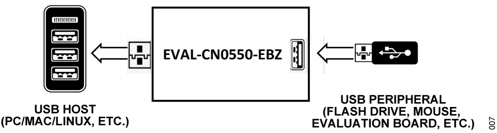
- Connect the EVAL-CN0550-EBZ to an available USB port on the host PC. The LEDs on the evaluation board should light up to indicate the presence of 5 V bus power on both host and peripheral sides.
- With the EVAL-CN0550-EBZ connected to the host PC, the connected peripheral should operate normally.
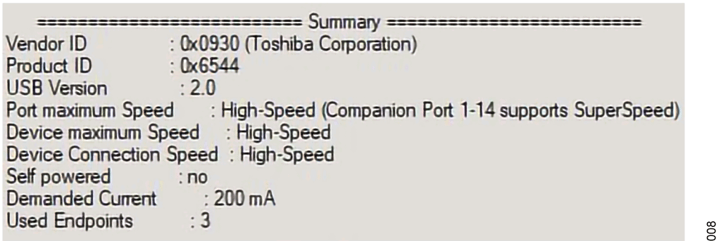
- Validate the speed of the connected peripheral using a USB device tree viewer (for Windows), the lsusb command (for Linux), or system profiler (for macOS). Figure 8 shows an example device tree of a high-speed USB device.
Discussions
Sample Products
Evaluation Boards
Pricing displayed is based on 1-piece.
Up to two boards can be purchased through Analog.com. To order more than two, please purchase through one of our listed distributors.
Pricing displayed is based on 1-piece. The USA list pricing shown is for budgetary use only, shown in United States dollars (FOB USA per unit), and is subject to change. International prices may vary due to local duties, taxes, fees and exchange rates.