


-
CN0585 User Guide5/23/2023WIKI
Overview
Design Resources
Design & Integration Files
- Schematic
- Bill of Materials
- Gerber Files
- Assembly Files
- Allegro Layout File
Evaluation Hardware
Part Numbers with "Z" indicate RoHS Compliance. Boards checked are needed to evaluate this circuit.
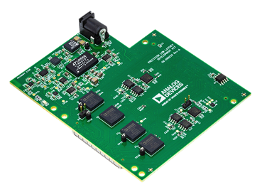
- EVAL-CN0585-FMCZ ($650.00) 4-Channel, Simultaneous Sampling, Data Acquisition Platform
Device Drivers
Software such as C code and/or FPGA code, used to communicate with component's digital interface.
FPGA/HDL
Features & Benefits
- 4 Analog Input Channels with Configurable Voltage Ranges
- 4 Analog Output Channels with Configurable Voltage Ranges
- 200 ns Latency between ADC Measurement and DAC Settling
- Analog Front End Interface Connector
- Modeling and Simulation Compatible with MATLAB and Python
- FMC Connector Interface to FPGA
Documentation & Resources
-
Solutions For Rapid Prototyping: Answering the Needs of Practicing Engineers8/23/2023PDF784 K
Circuit Function & Benefits
As modern electronic, electromechanical, and electro-optical systems continue to shrink in size, require faster response times, and have more stringent accuracy requirements, performance of the data acquisition and hardware-in-the-loop (HIL) systems required to develop and test these systems must keep pace.
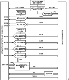
The circuit shown in Figure 1 consists of four 16-bit analog-to-digital (ADC) channels and four 16-bit digital-to-analog (DAC) channels that are interfaced with a field programmable gate array (FPGA) through a low pin count (LPC) FPGA mezzanine card (FMC) connector, providing a complete real-time precision data acquisition and signal generation platform with on-board power rails, voltage monitoring, logic level translation, general purpose I/O, I2C, SPI, and an application-specific analog front-end (AFE) interface connector.
A full capture and conversion of up to four simultaneous differential analog input signals at 15 MSPS can be performed in under 100 ns, with pin configurable input voltage ranges of ±10 V, ±5 V, ±4.096 V, ±2.5 V, and ±1.5 V.
Four analog output channels are provided using two dual 33 MSPS DACs with pin-configurable output voltage ranges of 0 V to +2.5 V, 0 V to +5 V, ±5 V, and ±10 V, enabling full-scale settled analog outputs to be generated in under 200 ns from initial data write to the DACs. Four simultaneous outputs can be generated at 15 MSPS or two can be generated at 30 MSPS. Analog bandwidth up to 5 MHz is supported for both signal acquisition and generation
The software interface is through the Linux industrial input/output (IIO) framework, providing a host of debug and development utilities and cross platform application support. Software templates are available in popular programming languages like Python and MATLAB® to enable customized signal generation and data acquisition. Hardware description language (HDL) templates are available to facilitate the addition of custom functionality.


Circuit Description
ANALOG INPUTS
The CN0585 can accommodate analog input ranges of ±10 V, ±5 V, ±4.096 V, ±2.5 V, and ±1.5 V by utilizing pin-configurable input attenuation and gain settings. Table 1 shows the pin configuration for each input range. Each of the four ADC input channels can be independently configured to any of the available input voltage ranges.
| Input Range | Differential Input Signal Connections | Feedback Connections |
| ±10 V | IN2P, IN2N | OUTP shorted to IN1N OUTN shorted to IN1P |
| ±5 V | IN1P, IN1N | OUTP shorted to IN2N OUTN shorted to IN2P |
| ±4.096 V | IN2P, IN2N | No connect |
| ±2.5 V | IN1P, IN1N | No connect |
| ±1.5 V | IN1P shorted to IN2P, IN1N shorted to IN2N |
No connect |
ANALOG-TO-DIGITAL CONVERSION
The CN0585 board features four ADAQ23876 16-bit 15 MSPS data acquisition μModules® providing simultaneous, synchronized acquisition of four differential input channels. Each channel's voltage range can be independently configured through the six input pins. Figure 2 shows the functional diagram of the ADAQ23876, including the six input selection pins shown in Table 1.


Voltage Reference
The default ADC reference configuration uses the internal 2.048 V, ±0.1% accurate, 20 ppm/°C max voltage reference. For more stringent use cases where the accuracy and temperature drift is an issue, an external LTC6655 2.048 V, ±0.025% accurate, 2 ppm/°C max voltage reference can be used.
DIGITAL-TO-ANALOG CONVERSION
The CN0585 board contains two AD3552R 16-bit 33 MSPS DACs, providing four analog output signals to the AFE connector. Each DAC output voltage range can be individually selected using the pin configurations shown in Table 2.
For each output voltage range option, the minimum and maximum output voltages are set 1.5% higher and lower than the listed values. This ensures that the desired full-scale or zero-scale amplitude within that range can be generated without signal clipping. In addition to the pin configurations, the DAC device register settings must be changed to match the output voltage range selected. These register settings can be updated using the provided software interfaces.
| Output Range | Range Configuration Connections |
| ±10 V | DACx to DACx_RFB0 |
| ±5 V | DACx to DACx_RFB0_X2 |
| 0 V to 10 V | DACx to DACx_RFB0_X2 |
| 0 V to 5 V | DACx to DACx_RFB0_X1 |
| 0 V to 2.5 V | DACx to DACx_RFB0_X1 |
Figure 3 shows the functional diagram of the AD3552R, including the output voltage range configuration pins shown in Table 2.


Voltage Reference
The default DAC reference configuration uses the internal 2.5 V, ±0.3% accurate, 10 ppm/°C max voltage reference. For more stringent use cases where the accuracy and temperature drift is an issue, an external ADR4525 2.5 V, ±0.02% accurate, 2 ppm/°C max voltage reference can be used.
DIGITAL INTERFACE
The CN0585 relies on external clock signals provided through the FMC interface to operate. Figure 4 shows the digital interface between the ADC/DAC components and the FMC connector.
Each of the four ADC channels requires a low voltage differential signaling (LVDS) interface consisting of a differential CLK, DA, DB, and DCO signals. Each pair of DAC channels requires a quad SPI interface consisting of CS, SCLK, SDO0, SDO1, SDO2, SDO3, and LDAC signals. The signals are made available on the FMC connector and are intended to interface with an external FPGA board.


The CN0585 FPGA firmware synchronizes ADC acquisitions from multiple channels, as well as provides analog feedback from the DAC outputs, with minimal latency. Special care must be taken to ensure CNV signals and clocks are synchronized between channels and that clocking can support 15 MSPS to ensure low latency feedback.
AD3552R Quad SPI Mode
Data is transferred to the AD3552R DACs from the FPGA through the FMC LPC connector using a quad serial peripheral interface (QSPI) dual data rate interface.
In quad SPI mode, the SDI/SDIO0, SDO/SDIO1, SDIO2, and SDIO3 data lines are bidirectional, as shown in Figure 5. During the data phase, the R/W bit of the instruction phase defines the direction of the data lines. During the instruction phase, the data lines are always configured as inputs. In quad SPI mode, consecutive bits are serialized in groups of four, as shown in Figure 6.


ADAQ23876 LVDS Interface
In Figure 7, the ADAQ23876 conversion is controlled by the CNV+ and CNV– inputs, which are driven directly with an LVDS signal. A rising edge on CNV+ samples the analog inputs and initiates a conversion.


At high sample rates, the required LVDS interface data rate can reach >400 Mbps. Most FPGAs can support this rate, but if a lower data rate is desired, the two-lane output mode can be used. When the TWOLANES input pin is connected high (VIO), the ADAQ23876 outputs two bits at a time on DA-/DA+ and DB-/DB+, as shown in Figure 8.


POWER TREE
The primary power for the CN0585 is provided by the USB-C PD power adapter, which must supply at least 12 V and up to 1.5 A. A MAX77958 USB-C power delivery controller configures the power adapter to deliver 20 V. The complete power tree can be seen in Figure 9.


The LTM8078 dual output step-down converter provides 10 V and 5.5 V outputs, which supply the remainder of the power tree.
The LTM8049 dual channel inverting DC/DC converter outputs +15 V and -15 V rails, which are used to feed further power stages and are made available at the AFE connector.
The LT3045 and LT3094 ultralow noise, low dropout (LDO) regulators provide +12 V and -12 V rails, respectively, which provide the supply voltages for the AD8065 FastFET™ op amps at the DAC outputs and which are also made available at the AFE connector.
The LT3032 low noise, LDO regulator provides +5 V and -5 V supply voltages for the internal amplification stage of each ADAQ23876.
The ADP223 low noise regulator provides the 5 V supply voltages for the ADCs and DACs.
The LTM8074 step-down regulator provides a 2.5 V output to the ADP122 and ADP124 low quiescent current linear regulators, which in turn, provide the digital supply voltages for the DACs and ADCs, respectively.
The USB-PD -15 V, -12 V, +12 V, and +15 V power rails described above are made available at the AFE connector. Additionally, a +3.3 V rail is fed through from the FPGA FMC connector to the AFE connector.
VOLTAGE MONITORING
The CN0585 provides voltage monitoring on important power rails to ensure the board is operating properly. These monitored values are measured using an AD7291 12-bit, 8 channel ADC and a resistive divider network, which is shown in Table 3. The full list of monitored rails includes the ±12 V DAC amplifier rails, the ±5 V ADC amplifier rails, the 5 V analog ADC and DAC rails, and the 1.8 V and 2.5 V digital ADC and DAC rails.
| RF Device | CN0585 Power Rail | Measured Voltage | Actual Voltage |
| voltage0 | +12 V (AD8065 DAC amp) | 2.26 V | 12 V |
| voltage1 | -12 V (AD8065 DAC amp) | 0.65 V | -12 V |
| voltage2 | +5 V (ADAQ23876 internal amp) | 2.06 V | 5 V |
| voltage3 | -5 V (ADAQ23876 internal amp) | 0.76 V | -5 V |
| voltage4 | +5 V (DAC) | 2.06 V | 5 V |
| voltage5 | +5 V (DAC) | 2.06 V | 5 V |
| voltage6 | +2.5 V (digital) | 2.25 V | 2.5 V |
| voltage7 | +1.8 V (digital) | 1.80 V | 1.8 V |
SYSTEM PERFORMANCE
Latency
Figure 10 shows the latency and settling time of the CN0585 output as captured by an oscilloscope. With the CN0585 DAC output set to ADC input mode, a pulse (shown in red) was applied to one of the ADC channel inputs, and the corresponding DAC channel output (shown in blue) was monitored. The latency from the measured input signal to the DAC output signal beginning to rise was approximately 250 ns; 50 ns of this delay is attributed to the internal FPGA data processing, while the remaining 200 ns of the delay is attributed to ADC data capture and DAC update.


Analog Input Performance
The analog signal acquisition path of the CN0585 exhibits very high spurious-free dynamic range (SFDR). Figure 11 shows a 16K point FFT of the ADC’s data at a sample rate of 15 MSPS, with a 1 kHz, ±10 V sinusoidal input signal. The CN0585 achieves 105 dB of SFDR, dominated by the 3rd harmonic. All other spurs are lower than 120 dBC across the full 7.5 MHz input frequency range.


Figure 12 shows the input frequency response of the ADC.


Output Filtering
A low pass filter is present at the output of each DAC. Figure 13 shows the frequency response of the filter as measured to 7.5 MHz with the ADC output used as the DAC input.


Figure 14 shows the frequency response of the output, with ideal waveforms generated in software, loaded into a cyclic buffer, and written to the DAC. Slightly less attenuation is seen in this plot due to the lower latency when compared to the full loopback measurement, which must pass samples to the FPGA and back.


Analog Output Linearity
The linearity of the CN0585 analog output is directly resultant from that of the AD3552R DAC. Figure 15 shows the integral nonlinearity (INL) of the DAC plotted against its full range of codes measured at 25°C. The DACs are intended to operate at 30 MSPS, so expected performance would be similar to 33 MSPS.


Figure 16 shows the differential nonlinearity (DNL) of the DAC measured at 25°C.


LAYOUT CONSIDERATIONS
For all high speed layouts carrying sensitive analog signals like the CN0585, it is important to follow the recommended printed circuit board (PCB) design practices for both low noise analog and digital high speed circuits. These include minimizing trace lengths, separating or shielding analog signals from high speed digital signals, using solid ground planes under signal traces, and minimizing via usage on sensitive analog and high speed digital traces.
The CN0585 PCB is a 10-layer design, utilizing several ground planes to separate analog, high speed digital, low speed digital, and power delivery signals. Careful consideration must be given to match the separate signals classes with solid ground plane returns. All clock and data lines to and from the ADCs and DACs should be routed as 100 Ω differential pairs and be length-matched between channels to within 10 mm to minimize timing skew to less than 75 ps.
Trace lengths from the ADC and DAC devices should be minimized to achieve a propagation delay of less than 0.5 ns from the devices to the FMC connector. Analog trace lengths from the AFE interface connector to the ADC inputs and DAC outputs should be minimized to reduce interference from external sources and minimize any gain errors from the input and output range configuration resistors.
SIMULATION AND MODELING
Simulink® can be used to create custom HDL models, which can be loaded into the FPGA and run in real time using the CN0585. Algorithms can be used to implement control systems, perform digital signal processing (DSP) operations on measured signals, or emulate hardware functions.
Figure 17 shows the placement of a Simulink model inserted in both receive and transmit signal paths within the CN0585 block diagram. This means that ADC samples are passed through the HDL model and stored into memory and that DAC samples are passed through the HDL model and output to the AFE connector. HDL models can also be inserted in receive-only or transmit-only signal paths, which provides access exclusively to ADC inputs or DAC outputs, respectively.


For any receive signal path models inserted, the modified samples can be accessed using Python, MATLAB®, or by viewing them using the IIO Oscilloscope software as shown in Figure 18.


Common Variations
The AD3542R DAC can be used in place of the AD3552R for applications where a maximum of only two 15 MSPS channels are required and an increase in small signal settling time of ~20% is tolerable at a lower system cost and footprint area.
The discrete LTC2387-16 ADC can be used in place of the ADAQ23876 in order to configure alternate input voltage ranges. For applications requiring higher resolution, the LTC2387-18 can be used instead.
Circuit Evaluation & Test
This section covers the setup and procedure for evaluating the EVAL-CN0585-FMCZ. For complete setup details and other important information, refer to the CN0585 User Guide.
For a full functional test setup and results, refer to the CN0584 circuit note.
EQUIPMENT NEEDED
Required Hardware
- CN0585 circuit evaluation board (EVAL-CN0585-FMCZ)
- Zedboard Xilinx Zinq development board
- 16 GB SD card
- Micro-USB cable
- USB-C wall adapter
- Ethernet cable
- Host PC (Windows or Linux)
- Oscilloscope
Required Software
GETTING STARTED
- Flash an SD card with the Analog Devices Linux Kuiper image.
- Configure the SD card with the appropriate boot files.
- Connect the Zedboard to the EVAL-CN0585-FMCZ.
- Connect the power supply to the EVAL-CN0585-FMCZ.
- Connect the Ethernet cable and the UART micro-USB cable to Zedboard, and the other ends to the host PC.


FUNCTIONAL TEST SETUP
- Launch IIO Oscilloscope and connect to the Zedboard, as shown in Figure 20.


- In IIO Oscilloscope, set the AD3552R DAC output ranges to ±10 V and the input source to dma_input as shown in Figure 21.


- Navigate to the DMM tab of IIO Oscilloscope and confirm that the voltage monitor values align with those shown in Figure 22.


- Navigate to the DAC Data Manager and load the provided sinewave_0.3.mat sample waveform to each DAC output channel as shown in Figure 23.


TEST RESULTS
After following the steps in the test setup, each DAC channel should be outputting a 150 kHz sinusoidal signal. Use the oscilloscope to probe each of the four DAC output test points, which are labeled TP1 to TP4, and confirm that the waveform is present.
Discussions
Sample Products
Evaluation Boards
Pricing displayed is based on 1-piece.
Up to two boards can be purchased through Analog.com. To order more than two, please purchase through one of our listed distributors.
Pricing displayed is based on 1-piece. The USA list pricing shown is for budgetary use only, shown in United States dollars (FOB USA per unit), and is subject to change. International prices may vary due to local duties, taxes, fees and exchange rates.