


Overview
Design Resources
Design & Integration Files
- Schematic
- Bill of Materials
- Gerber Files
- Assembly Files
- Layout File
Evaluation Hardware
Part Numbers with "Z" indicate RoHS Compliance. Boards checked are needed to evaluate this circuit.
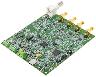
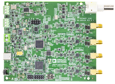
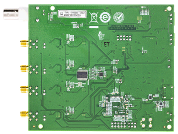
- EVAL-CN0582-USBZ ($750.00) USB 3.0 Quad-Channel IEPE Vibration Sensor Measurement System
- SW-CN0582-API ($10000.00) CN0582 Application Programming Interface
Device Drivers
Software such as C code and/or FPGA code, used to communicate with component's digital interface.
Features & Benefits
- 4-Channels of Analog Input
- IEPE, 4-20mA Sensor Compatible
- Frequency Generator Output
Documentation & Resources
-
CN0582: USB 3.0 Quad-Channel IEPE Vibration Sensor Measurement System (Rev. A)11/22/2022PDF731 K

Circuit Function & Benefits
Integrated electronics piezoelectric (IEPE) and IEPE-compatible accelerometers and velocity sensors are used in a wide array of condition-based monitoring (CbM), building monitoring, and structural analysis applications. Often multiple channels are used to measure 3-dimensional acceleration at a single location, or multiple 1-dimensional measurements at several locations.
Benchtop data acquisition (DAQ) systems are applicable in research and calibration environments, however these usually come in sizes and at costs that are not conducive for direct integration into end applications.
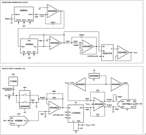
The circuit shown in Figure 1 is a self-contained, USB-based quad-input channel IEPE data acquisition system. The four channels are simultaneously sampled with 24-bit resolution and have a sample rate of up to 256 kSPS. The signal chain is dc-coupled, providing frequency response to 0 Hz, while a dc offsetting circuit maximizes the dynamic range. Each input channel includes a constant current source for powering standard IEPE sensors. All data signals and power rails are derived from a single USB 3.0 connection.
The system also includes an on-board direct digital synthesis (DDS) signal generator, which can be used for electrical calibration or as an excitation source to a shaker table or vibration calibrator for sensor and system-level calibration.
Data can be captured and analyzed with the companion software application, and custom software can be developed using the provided application programming interface (API).

Circuit Description
The CN0582 is a complete solution capable of measuring data from analog sensors using the provided software or API libraries.
The system offers a variable amplitude and frequency sinusoidal signal to drive an external shaker table as a test stimulus for reading back different sensor responses.
The solution comes with evaluation software that provides full control over all the board’s functions. These functions include enabling current sources and ac- or dc-coupling, input bias adjustment, data capture in both time and frequency domain, providing a single-tone or sweeping sinusoid, and data export.
The optional software API library is compatible with many different environments, and was tested using LabVIEW, C#, and Python. The API enables customers to develop their own custom functions and complete applications.
Several key features of this solution are as follows:
- 4-channel simultaneous data acquisition
- On-board IEPE excitation
- IEPE input channel offsetting
- Signal Generator:
- Single tone or linear sweep
- Electronic loopback testing
- Shaker table excitation
- CN0582 Evaluation Software
- System configuration
- Graphical display
- File export (data acquisition, vibration test)
| Specifications | Min | Typ | Max | Unit/Remarks | |
| Power Requirements | |||||
| Input | Voltage | 4.5 | 5 | 6 | V |
| Current | 500 | 600 | mA | ||
| Analog Input | |||||
| IEPE | Full scale | 0.1m* | 10 | V | |
| Bias | 13 | VDC |
|||
| Current source | 4 | mA | |||
| 4 mA to 20 mA (CH3) | Resistance | 249 | Ω | ||
| Power | 0.25 | W | |||
| THD + N | -87 | -84 | dB, 3.3 Vp-p at 1 kHz | ||
| SNR | 99 | dB, 10 Vp-p at 20 Hz to 20 kHz | |||
| Accuracy | 1 | % error (at greater than 100 mV) | |||
| Analog Output | |||||
| Voltage | 0.5 |
7 | V peak-to-peak | ||
| Frequency | 0.02 |
25 | kHz | ||
| THD + N | -52 | -55 | dB, 7 Vp-p at 20 Hz to 20 kHz | ||
| Accuracy | 1 | % error | |||
*Based on PGA setting of 1.
VIBRATION SENSOR TYPES
Piezo vs. MEMS Sensor
Traditionally, piezoelectric accelerometers have been the benchmark for vibration monitoring and are still the sensor of choice in the highest sensitivity applications, or where very high accelerations are involved. Microelectromechanical systems (MEMS) sensors were previously deemed unusable due to their limited bandwidth, g-range, and noise performance across frequency.
Recent advancements in MEMS sensor technology (especially with frequency response and noise performance) make MEMS sensors a viable alternative in many CbM applications. MEMS sensors are typically smaller and lower cost, and have a frequency response that extends to dc (0 Hz). One example is the CN0532, a typical MEMS based sensor with circuitry implementing an IEPE interface.
The CN0582 is compatible with piezoelectric IEPE sensors as well as IEPE-compatible sensors based on other technology. The excitation current sources can be disabled, allowing connection to voltage output sensors.
IEPE INTERFACE
Unconditioned piezoelectric sensors have a high output impedance, making it difficult or impossible to drive any length of cable. These sensors are also sensitive to cable movements and electromagnetic interference, and require precision, high impedance signal conditioning circuitry.
IEPE refers to a standard in which the signal conditioning electronics are integrated into the sensor. The internal electronics convert the high impedance charge output into a low impedance voltage signal, making it easier to transmit. The standard also uses a single conductor to provide both power and signal, which minimizes cabling complexity.
Figure 2 shows a high level block diagram of the IEPE interface. Power is supplied via a constant current source to the sensor. The sensor then modulates the output voltage depending on the measured vibration, which allows the signal to be measured across the same line as the power source.


IEPE Excitation and Control
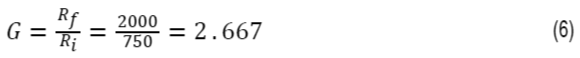
IEPE sensors require power in the form of a constant current source to operate properly. Aside from the constant current ranging from 2 mA to 20 mA, the source must have a compliance of 24 V to 30 V, which is at least twice the typical IEPE bias voltage of 8 V to 12 V. Figure 3 shows the IEPE high voltage, constant current source topology based on the LT3092.


Using the formula shown in Equation 1, the constant current source for the CN0582 is set to 4 mA.

where:
IOUT is the constant current output.
ROUT is the current output set resistance.
RSET is the current input set resistance.
The current source can be enabled or disabled by an ADG5401, a high voltage, low resistance switch.
Commands sent from the software to the board toggle the corresponding channel to the desired state.
Powering the ADG5401 from the same 26 V supply as the current sources ensures that the input voltage remains within limits, while the 6.5 Ω on-resistance is small enough to have an effect on the signal level.
When the current source is disabled, the input for each channel acts as a typical high impedance voltage input analog-to-digital converter (ADC) measurement. Channel 3 features an on-board load resistor that allows the user to connect and measure the data from a 4 mA to 20 mA sensor, whose value can be computed using Equation 2:

where:
VSENSOR is the converted sensor voltage.
RLOAD is the load resistor (249 Ω).
ISENSOR is the sensor output current.
Input Protection
To avoid overdriving any part of the input circuitry, transient voltage suppressor (TVS) diodes are added at the input connector. These diodes ensure that the input can withstand voltages up to 40 V, protecting the sensitive analog input circuitry from dangerous voltage levels.
AC/DC Coupling
Depending on the sensor, either ac-coupling or dc-coupling may be more appropriate. DC-coupling is applicable for sensors with a response that extends to zero Hz, and that have a small, or well-specified offset voltage. AC-coupling is more appropriate for sensors that inherently have a highpass response, and may have a large dc offset that varies over operating conditions.
Figure 4 shows the ac- and dc-coupled paths, controlled by an ADG5436 high voltage, latch-up proof, dual SPDT switch.


The switch is powered from a bipolar -5 V or 26 V supply, which accommodates typical IEPE sensor outputs, as well as voltage output sensors with 0 V to 5 V, ±5 V, and 0 V to 10 V ranges. The ac-coupling path is composed of a high pass filter, whose cutoff frequency can be calculated using Equation 3:

where:
fc is the high pass cutoff frequency.
IEPE Input Offsetting
IEPE signals naturally have a high dc bias and peak-to-peak values, making it difficult to interface with common smaller range converters. To overcome this challenge, a level shifting circuit is used.
Figure 5 shows the level shifter implementation based on the ADA4522. The attenuation and voltage shift are designed to utilize the full ±4.096 V ADC input range by centering the input as close as possible to zero.


The required voltage shift is calculated using Equation 4:

where:
VSHIFT is the level shift voltage.
VIEPE_INPUT is the input bias voltage.
VIEPE_SHIFTED is 2.52 (must be equal to VOCM).
G is 0.3 (computed as RFB/RIN).
The level shift voltage (VSHIFT) is provided by the AD5686R digital-to-analog converter (DAC). The value of VSHIFT can be programmed using Equation 5:

where:
VSHIFT is the level shift voltage.
VREF is the voltage reference of AD5686R.
Gain is the gain setting of AD5686R.
D is the digital code.
N is the number of bits of AD5686R (16-bit).
PROGRAMMABLE GAIN AMPLIFIER (PGA)
Aside from the input signal coupling and level shifting options, the CN0582 also provides additional gain for smaller input signals. The gain can be set for each individual analog input channel.
Figure 6 shows the PGA implementation using the LTC6910. The common-mode voltage from the other signal conditioning stages is connected to the AGND pin, which serves as the reference for amplification.


Depending on the gain option selected, the valid input range for the CN0582 also changes. Table 2 describes the acceptable input voltage range for each gain setting; voltages outside the valid input range result in signal distortion and clipping.
| PGA Settings | Maximum AC Input |
| 1 | 10 Vp-p |
| 2 | 5 Vp-p |
| 5 | 2 Vp-p |
| 10 | 1 Vp-p |
| 20 | 500 mVp-p |
| 50 | 200 mVp-p |
| 100 | 100 mVp-p |
Note: The system can measure signal amplitudes of 100 μVp-p, but the signal-to-noise ratio (SNR) is compromised. Thus, the recommended minimum input amplitude is 500 μVp-p.
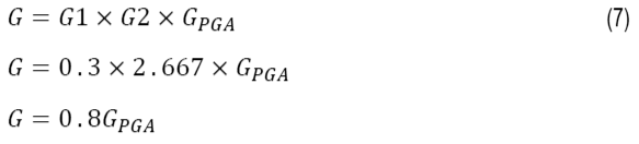
FULLY DIFFERENTIAL AMPLIFIER (FDA)
Since the output signal of the PGA is a pseudo-differential signal with a common-mode of 2.5 V, it needs to be amplified and converted to a fully differential signal to maximize the use of the ADC’s full scale input range of 8.192 Vp-p.
Figure 7 shows the ADA4945 fully differential ADC driver used to convert the pseudo differential signal from the PGA to a fully-differential signal for the ADC.


The PGA output with respect to VOCM is amplified and converted to a fully differential signal by the ADA4945 with a gain shown in Equation 6:
In case of over or undervoltage due to the input and gain combinations, the ADA4945 clamps the output to +VS or -VS to protect the succeeding sensitive ADC input stage.
OVERALL SIGNAL CHAIN GAIN
The total gain on the analog input path comes from the level shifter, FDA, and PGA, which can be computed using Equation 7:
G is the overall system gain of the CN0582.
G1 is the gain of the level shift attenuation (0.3).
G2 is the gain of the FDA (2.667).
GPGA is the programmable gain of the PGA (1, 2, 5, 10, 20, 50, 100).
The maximum allowable ac or dc voltage on the analog input path is directly related to the gain settings of each channel. Equation 8 shows how to calculate the dc input voltage, assuming a PGA gain setting of 1.

The maximum dc bias input voltage is:
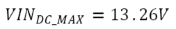
where:
VINDC_MAX is the maximum dc voltage into the CN0582.
VSHIFT_MAX is the AD5686R maximum output voltage (5 V).
G1 is the gain of the level shift attenuation (0.3).
VOCM is the AD7768-4 common-mode voltage (2.52 V).
The ac input voltage can be computed using Equation 9, assuming that the PGA gain setting is 1.

The maximum peak-to-peak input voltage swing is:
VINAC_MAX is the maximum ac input voltage into the CN0582.
VREF_ADC is the AD7768-4 internal voltage reference (4.096 V).
G2 is the gain of FDA (2.667)
G1 is the gain of the level shift attenuation (0.3)
The theoretical maximum ac input swing is 10.23 Vp-p, but the CN0582 is only tested up to 10 Vp-p to meet the headroom requirements of the amplifiers. The same logic applies to maximum dc bias, which was only tested to 13 VDC. Centering the ADC output around zero by adjusting VSHIFT implies the IEPE_SHIFTED signal is equal to VOCM.
DATA CAPTURE AND DIGITAL CONTROLLER
Analog-to-digital conversion is performed by an AD7768-4, a 4-channel 24-bit simultaneous sampling Σ-Δ ADC. It contains several power scaling, filter, and sample rate options to optimize for different constraints like noise, bandwidth, and power consumption.
The AD7768-4 acts as a source-synchronous transmitter, with each channel’s data serialized on one of four data lines. The data is received by the digital controller and streamed to the host computer over USB.
The digital controller is also responsible for configuring the analog input channels, enabling the current sources, setting the ADC modes, and setting up the waveform generator.
POWER SUPPLY ARCHITECTURE
The CN0582 is powered from a single USB 3.0 port providing 5 V at 900 mA, and several dc-to-dc converters produce the required voltage rails. The system power tree consists of boost converters followed by linear dropout regulators for the analog circuits to obtain the lowest possible noise, and buck converters for digital circuits for maximum efficiency. Figure 8 presents the complete power architecture of CN0582.


WAVEFORM GENERATION AND CONTROL
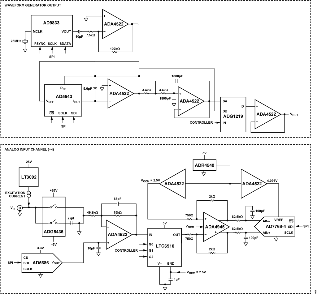
The CN0582 has an on-board waveform generator used to excite and control a shaker table, which helps in testing and calibrating IEPE sensors.
Figure 9 shows the block diagram utilizing the AD9833, a programmable waveform generator with a constant voltage output of 600 mVp-p and configurable frequency output from 0 Hz to 12.5 MHz with 28-bit resolution. The output frequency can be computed using Equation 10:

FOUT is the output frequency.
FREF is the reference clock frequency.
FREQ is the frequency register value.


The CN0582 frequency output is band limited to 25 kHz, which is adequate for most vibration and CbM applications. The output signal is then amplified and conditioned using the ADA4522 in a high pass filter configuration, which removes the dc offset, a requirement for many shaker table inputs.
The maximum set gain of ADA4522 can be computed using Equation 11:
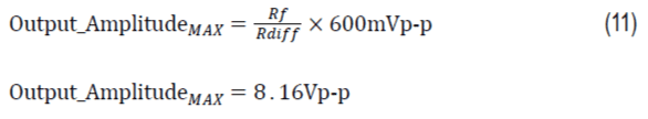
Output_AmplitudeMAX is the maximum amplitude set by the gain of the ADA4522.
Rf is 102 kΩ.
Rdiff is 7.5 kΩ.
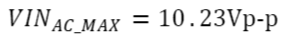
The signal generator can produce 8.16 Vp-p maximum, but the graphical user interface (GUI) limits the output voltage to 7 Vp-p.
The CN0582 signal generator output amplitude is controlled by an AD5543 current output DAC, configured in a current to voltage topology as shown in Figure 10.


The amplitude can be controlled following Equation 12:

Output_Amplitude is the modulated output amplitude.
D is the digital code value.
After configuring the desired output amplitude and frequency, an optional post-filtering circuit is available to reduce the broadband noise. The circuit uses the ADA4522 in a Sallen-key low pass filter configuration at the DAC's output, because of the stability and high input impedance characteristics. The cutoff frequency is set to 26 kHz, and can be computed using Equation 13:

The cutoff frequency is adjusted to at least twice the intended IEPE bandwidth of 10 kHz, so that negligible attenuation occurs.
The output selector stage shown in Figure 11 uses an ADG1219 switch between filtered and unfiltered output from the amplitude controller. The selected output is then buffered to isolate the circuit from the output connector.


Common Variations
The AD3552R 16-bit, 33 MSPS DAC is an alternative to the AD9833 with higher resolution, lower distortion, and arbitrary waveform generation capability, however it requires a data source.
The ADG5436F is a fault-protected variant of the ADG5436 that provides additional protection from input faults, as well as fault detection.
For the ADC, if the application needs to operate beyond the IEPE bandwidth, a good alternative is the AD4134. This device has a higher sampling rate and an improved overall performance.
A higher channel count system can also be realized by using the AD7768. The existing controller already has a provision for 8-channel inputs, making it relatively easy to increase the captured channels for the current system.
The CN0549 is a single-channel IEPE-compliant, CbM development platform geared toward software development.
Circuit Evaluation & Test
The circuit test and evaluation demonstration highlight the capabilities of the EVAL-CN0582-EBZ using C#-based Windows PC application. For complete details on using the hardware and software, check out the CN0582 User Guide.
EQUIPMENT NEEDED
- EVAL-CN0582-USBZ Evaluation Board
- CN0582 Evaluation Software
- Host PC (Windows)
- Vibration Shaker (9363-ED-2F4K-5N, King Design)
- Reference and Test Sensors (Reference: PCBM352C67)
- Audio Analyzer (Audio Precision© APX525)
- Oscilloscope (Rohde & Schwarz® RT1004)
- USB Type-C cable
- SMA cable
- BNC to BNC cable
GETTING STARTED
This section discusses the general procedure to set up the evaluation test for the EVAL-CN0582-USBZ.
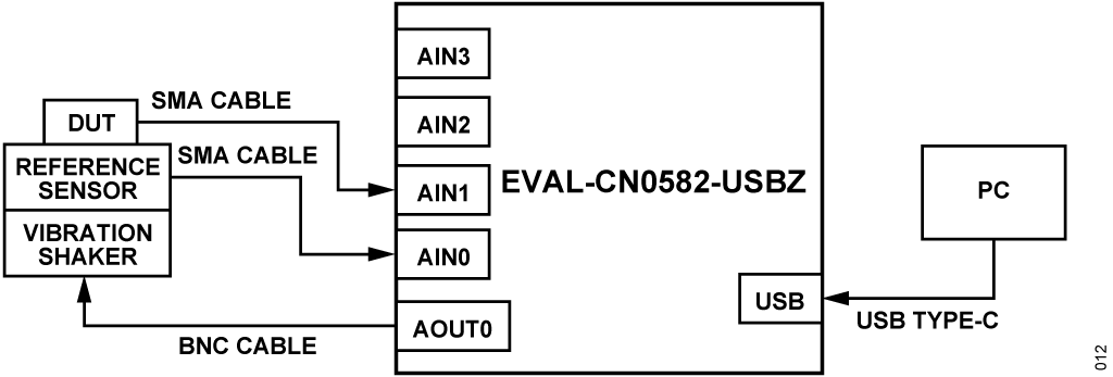
The setup requires the EVAL-CN0582-USBZ to be connected to a Windows PC, with the CN0582 evaluation software installed; and then to a vibration shaker, which acts as the stimulus for device under test (DUT) measurements, as displayed in Figure 12.
To test the basic functions of the board, follow these instructions:
- Install the CN0582 Evaluation Software to the Host PC based on the instructions listed in software installation guide.
- After installing the software, connect the EVAL-CN0582-USBZ board sensors to any of the analog inputs of using an SMA cable; following these channel assignments:
- CH0 for the Piezo reference sensor.
- CH1 to CH3 for the DUT sensors (IEPE, MEMS, etc).
- Connect USB Type-C cable to EVAL-CN0582-USBZ, and then plug it in to the Host PC.
- Open the software and for simple data capture, select DAQ from the window options as shown in Figure 13.


- Configure the software for the different settings required by the sensor such as input signal coupling, offset, and gain. Enter the recommended settings from Table 3 into the corresponding GUI fields shown in Figure 14.
| Current Source switch | ON for CH0, CH1 OFF for CH2, CH3 |
| Coupling | DC for all channels |
| Gain | x1 for all channels |
| Level Shift Voltage | 10500 to 13000 for each channel Adjust accordingly depending on the connected sensor per channel. |


- On the top right pane of the GUI, set the output parameters of the signal generator following the input values suitable for the vibration shaker as shown in Table 4.
| Amplitude | 500 mVp-p |
| Frequency | 1000 Hz |
- Under the 'Channel Selector' field, switch on CH0 and CH1 to display plots. Toggle the data capture 'Mode' button depending on the preferred plot results.
- Connect analog output of EVAL-CN0582-USBZ to the vibration shaker using a BNC to BNC cable.
Note: Connect the analog output to the vibration shaker only when the software has finished uploading the firmware to the EVAL-CN0582-USBZ to prevent damage to the instrument.
- Click the start button to begin capturing and viewing time and frequency domain data from the ADC.
ANALOG INPUT TESTING RESULTS
For input channel accuracy, a precision audio analyzer is used as input source of which percentage error must be less than 1% at any amplitude and frequency. Table 5 shows the measured values for four channels displayed in GUI corresponding to the test parameters from the equipment.
At amplitudes less than 100 mVp-p, the maximum error is ±2 mVp-p; while at above 100 mVp-p, the average error is less than 1%.
| DC BIAS = 6 V | Test Amplitude (mVp-p) at Gain = 1 | |||||
| 10 | 100 | 1000 | 5000 | 10000 | ||
| Test Frequency (kHz) |
0.1 | 10.96 | 100.60 | 1000.51 | 4996.04 | 9992.53 |
| 1 | 10.96 | 100.93 | 1000.70 | 4996.11 | 9993.93 | |
| 5 | 10.93 | 100.74 | 999.68 | 4991.07 | 9984.00 | |
| 10 | 10.93 | 100.48 | 996.35 | 4975.71 | 9953.88 | |
| 25 | 10.80 | 98.46 | 975.81 | 4871.66 | 9745.64 | |
ANALOG OUTPUT TESTING RESULTS
To assess the signal generator, the output waveform is measured using an oscilloscope. Similar with the input channels, the average error must be less than 1% at any amplitude and frequency setting. Table 6 shows the programmed frequency and amplitude of a sinusoidal waveform captured on the oscilloscope, resulting in an error within 1%.
| Signal Generation (Full Bandwidth) |
Test Amplitude (mVp-p) | |||||||
| 100 | 500 | 1000 | 2000 | 3000 | 3500 | 7000 | ||
| Test Frequency (kHz) |
0.1 | 100.2 | 500.6 | 1001 | 2000.6 | 2998 | 3492 | 6976 |
| 1 | 100.2 | 499.7 | 1004 | 1994 | 3004 | 3500 | 6988 | |
| 5 | 100 | 500.5 | 999.8 | 2000 | 2998 | 3502 |
6983 | |
| 10 | 100.5 | 502.4 | 1004 | 2007 | 3010 | 3520 | 6999 | |
| 25 | 100.1 | 504.7 | 1008 | 2014 | 3022 | 3526 | 6970 | |
| 50 | 102.5 | 512 | 1023 | 2042 | 3062 | 3285 | 6510 | |


Discussions
Sample Products
Evaluation Boards
Pricing displayed is based on 1-piece.
Up to two boards can be purchased through Analog.com. To order more than two, please purchase through one of our listed distributors.
Pricing displayed is based on 1-piece. The USA list pricing shown is for budgetary use only, shown in United States dollars (FOB USA per unit), and is subject to change. International prices may vary due to local duties, taxes, fees and exchange rates.