


-
CN0584 User Guide5/24/2023WIKI
Overview
Design Resources
Design & Integration Files
- Schematic
- Bill of Materials
- Gerber Files
- Assembly Files
- Allegro Layout File
Evaluation Hardware
Part Numbers with "Z" indicate RoHS Compliance. Boards checked are needed to evaluate this circuit.
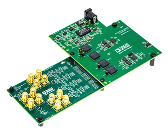
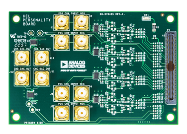
- EVAL-CN0584-EBZ ($200.00) Fault Protection, Hardware in the Loop Board
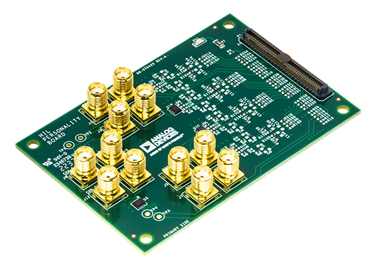
- EVAL-CN0585-FMCZ ($650.00) 4-Channel, Simultaneous Sampling, Data Acquisition Platform
Device Drivers
Software such as C code and/or FPGA code, used to communicate with component's digital interface.
FPGA/HDL
Features & Benefits
- 4 Analog Input Channels with Configurable Voltage Ranges
- 4 Analog Output Channels with Configurable Voltage Ranges
- 250 ns Latency between ADC Measurement and DAC Settling
- Analog Front End Board Modeling and Simulation Compatible with MATLAB and Python in Rx or Tx Paths
- All Power and Digital Connections provided by the Interface Connector
Markets and Technologies
Parts Used
Documentation & Resources
-
CN0584: Precision Low Latency Development Kit (Rev. 0)5/24/2023PDF1 M
Circuit Function & Benefits
As modern electronic, electromechanical, and electro-optical systems continue to shrink in size, require faster response times, and have more stringent accuracy requirements, performance of the data acquisition and hardware-in-the-loop (HIL) systems required to simulate, develop, and test these systems must keep pace. This is particularly true for applications requiring high power elements, such as the testing of motor controllers, linear actuators, generator controllers, electric vehicle chargers, or power grid elements for the automotive and energy industries. The increasing complexity of these modeled components leads to increased computation times, demanding faster solutions for signal acquisition and generation.
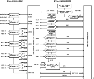
The circuit shown in Figure 1 is a complete precision low latency development kit, with 200 ns latency, and high-accuracy input bandwidth. This solution enables real-time HIL simulations and development of complex systems, significantly easing the design and testing of digital or mixed signal control loops. It is consists of four 16-bit analog-to-digital converter (ADC) channels and four 16-bit digital-to-analog converter (DAC) channels that allow synchronous acquisition of analog inputs and generation of output waveforms at 15 MSPS.
The development kit provides up to 5 MHz analog input bandwidth with extended analog and digital connectivity to simplify analog front end (AFE) design. Both the analog input range and output are hardware-selectable with five bipolar input ranges from ±1.5 V to ±10 V, and five output ranges from 5 V unipolar to ±10 V bipolar.
The software interface is available through the Linux industrial input/output (IIO) framework, providing a host of debug and development utilities and cross platform application support through Python, MATLAB®, C, C#, and other languages. The project integrates with Simulink®, where real-time models can be generated and loaded into the field programmable gate array (FPGA) board for testing with external hardware.


Circuit Description
HARDWARE-IN-THE-LOOP
The CN0584 simplifies and accelerates the development and test process for control systems using HIL emulation of expensive, complex, or not-yet-developed hardware. Figure 2 shows a high-level block diagram of a typical HIL setup using the CN0584 kit.


The electronic control unit (ECU) device under test (DUT) represents a controller, which produces digital output signals based on analog feedback inputs from the device it is controlling. The CN0584 emulates a device with custom hardware description language (HDL) loaded into an FPGA board, providing a real-time simulation of realistic performance.
One example of an HIL simulation that can be performed using the CN0584 is emulating the load for a 3-phase motor controller. The motor's behavior is first described in Simulink®, which is used to generate an HDL module that can be integrated into the CN0584 HDL template.
Applying this example to Figure 2, the ECU produces pulse width modulation (PWM) control signals, which are conditioned by three channels on the analog front end board and digitized by the ADCs on the data acquisition and signal generation board. Based on these inputs, the HDL hardware model simulates parameters such as the current draw, speed, inertia, and position of a modeled motor. These parameters are converted to analog signals and routed back to the ECU, which then closes the loop, adjusting its output PWM signals based on this feedback.
The ECU can be quickly evaluated for nominal operating conditions, corner cases (for example, maximum and minimum motor load), and various failure modes, each of which can be quickly implemented in simulation with no additional associated costs or damage to physical hardware.
ANALOG MEASUREMENT AND SIGNAL GENERATION
Input Voltage Range
The CN0584 supports an analog input voltage range of ±10 V by default. Additional input ranges of ±5 V, ±4.096 V, ±2.5 V, and ±1.5 V are hardware-selectable.
Analog Input Protection
The CN0584 provides analog input protection on all four ADC and DAC channels using the ADG5421F high voltage dual single-pole, single-throw (SPST) switch, offering overvoltage protection up to ±60 V. This protection is particularly important for HIL applications where high power signals may be present, and it also enables users to quickly adapt or modify their setups without worrying about miswiring or improper connections.
The ADG5421F is supplied by the +15 V and -15 V power rails, and if either the S1 or S2 pin exceeds one of those voltage levels by VT (0.7 V), the switch automatically turns off. For the ADCs, these pins connect to the differential input ports; and for the DACs, they connect to the two DAC channel output ports.
The ADG5421F also provides a fault flag (FF), which is routed to the CN0585 and read by a MAX7301 serial peripheral interface (SPI), 28-port I/O expander. The expander’s SPI port is routed to the FMC connector, and read by the FPGA board. In normal operation, the FF pin is pulled high. However, if an overvoltage condition is detected, the FF pin is pulled low to indicate a fault has occurred.
Output Voltage Range
The CN0584 supports an analog output voltage range of ±10 V by default. Additional output ranges of ±5 V, 0 V to +2.5 V, 0 V to +5 V, and 0 V to +10 V are hardware-selectable. Note that the register settings, which are controlled using the provided software interfaces, must also be updated for these output range modifications to take effect.
SYSTEM PERFORMANCE
Latency
Figure 3 shows the test setup used to measure the latency of the CN0584. A 1 MHz pulsed sine wave was generated from memory using the FPGA and passed through to one DAC output channel. This DAC output was monitored using an external scope and fed back via subminiature version-A (SMA) cable as an input to one of the ADC channels, where it was used as the input signal to the corresponding DAC channel. The output from this DAC channel was measured using the same oscilloscope, enabling the measurement of signal latency through the ADC input path, FPGA board, and DAC output path.


Figure 4 shows the latency and settling time of the CN0584 output as captured by an oscilloscope. With the CN0584 DAC output set to ADC input mode, a pulse was applied to one of the ADC channel inputs, and the corresponding DAC channel output was monitored. The latency from the measured input signal to the DAC output signal beginning to rise was approximately 250 ns; 50 ns of this delay is attributed to the internal FPGA data processing, while the remaining 200 ns of the delay is attributed to ADC data capture and DAC update.


Analog Input Performance
The analog signal acquisition path of the CN0584 exhibits very high spurious-free dynamic range (SFDR). Figure 5 shows a 16K point FFT of the ADC's data at a sample rate of 15 MSPS, with a 1 kHz, ±10 V sinusoidal input signal. The CN0584 achieves 105 dB of SFDR, dominated by the 3rd harmonic. All other spurs are lower than 120 dBc across the full 7.5 MHz input frequency range.


Figure 6 shows the same spectrum plot over a frequency range extending to 1 MHz, showing that no other harmonics or spurs over -120 dBm are present.


Figure 7 shows the input frequency response of the ADC.


Output Filtering
A low pass filter is present at the output of each DAC. Figure 8 shows the frequency response of the filter as measured to 7.5 MHz, with the ADC output used as the DAC input.


Figure 9 shows the frequency response of the output path, with ideal waveforms generated in software, loaded into a cyclic buffer, and written to the DAC. Slightly less attenuation is seen in this plot due to the lower latency when compared to the full loopback measurement, which must pass samples to the FPGA and back.


POWER ARCHITECTURE
All power for the CN0584 is provided by the CN0585 through the AFE connector.
The CN0584 uses the +15 V and -15 V rails to provide the positive and negative supply voltages for the ADG5421F input protection switches. The +12 V and -12 V rails provide the positive and negative supply voltages for the ADA4898-1 ADC buffer amplifiers. The +3.3 V rail powers the EEPROM circuit.
SOFTWARE OVERVIEW
Python
The CN0584 can be interfaced to Python using the pyADI-IIO library, which enables device configuration, capture of incoming samples from the ADCs, and generation of waveforms to be transmitted by the DACs. The output waveforms can then be pre- or post-processed based on ADC data, allowing a user to quickly and easily implement control loops or simulations of other hardware. Figure 10 shows an arbitrary waveform generated using Python and written to the DAC output. This example shows the generation of a ±10 V peak-to-peak 5 kHz sine wave, but any waveform can be implemented. For example, for an HIL setup one can generate a damped sine wave, chirp, noise, or distorted waveform to simulate defective hardware.


Figure 11 shows the measured input waveform for analysis, plotting the sine wave generated in Figure 10. The samples read from the ADCs can be processed and used as inputs to user-implemented Python algorithms implementing control loops, hardware emulations, or any other desired feedback systems.


MATLAB and Simulink
MATLAB® can also be used to interface with the CN0584 using the High Speed Converter Toolbox, which enables largely the same set of features as described for Python above. In addition to this, Simulink® can be used to create custom HDL models which can be loaded into the FPGA and run in real time using the CN0584. Existing Simulink models or custom algorithms can be used to implement control systems, perform digital signal processing (DSP) operations on measured signals, or emulate hardware functions. Figure 12 shows the placement of a Simulink model inserted in both receive and transmit mode within the CN0584 block diagram. This means that ADC samples are passed through the HDL model and stored into memory and that DAC samples are passed through the HDL model and output on the CN0584. HDL models could also be inserted in receive-only or transmit-only modes, which gives access exclusively to ADC inputs or DAC outputs, respectively.


For any receive signal path models inserted, the modified samples can be accessed using Python or MATLAB®, or viewed using the IIO Oscilloscope software.
Common Variations
Variations are possible on both the data acquisition and signal generation board and AFE board. For variations on the signal acquisition and generation paths, refer to the CN0585 circuit note.
The CN0584 allows a wide array of variations to tailor functionality to a specific application. A non-exhaustive set of examples is provided, but many additional possibilities exist and can be implemented to create any desired setup for HIL testing or other applications.
Bypassing the ADA4898 input buffer amplifier is possible for applications not requiring high input impedance. For higher speed applications where amplifier bandwidth is critical and slightly higher noise can be tolerated, the ADA4895 can be used in its place. For applications where high bandwidth is not as essential but a wider input voltage range is desired, the LTC6373 can be used. Alternatively, the ADA4255, which includes overvoltage protection, can be used for similar applications to replace both the ADA4895 and ADG5421F.
Application-specific variations are possible on the DAC output path as well. For example, for high voltage operations, the ADHV4702 which can drive outputs up to ±110 V, can be added to the output signal path.
Circuit Evaluation & Test
This section covers the setup and procedure for evaluating the EVAL-CN0584-EBZ. For complete details and other important information, refer to the CN0584 User Guide.
EQUIPMENT NEEDED
Required Hardware
- EVAL-CN0584-EBZ
- EVAL-CN0585-FMCZ
- Zedboard Xilinx Zinq development board
- 16 GB SD card
- Micro-USB cable
- USB-C wall adapter
- Ethernet cable
- 4x SMA cables
- 4x SMA 50 Ω terminations
- Host PC (Windows/Linux)
Required Software
- UART terminal capable of 115200 baud rate (recommended PuTTY)
- IIO Oscilloscope
- Analog Devices, Inc. Kuiper Linux image
GETTING STARTED
- Flash an SD card with the Analog Devices Linux Kuiper image.
- Configure the SD card with the appropriate boot files.
- Attach the EVAL-CN0584-EBZ to the EVAL-CN0585-FMCZ through the AFE connector.
- Connect the Zedboard to the EVAL-CN0585-FMCZ using the FMC connector.
- Connect the power supply to the EVAL-CN0585-FMCZ.
- Connect the Ethernet cable and the UART micro-USB cable to Zedboard, and the other ends to the host PC.
- Connect the EVAL-CN0584-EBZ analog I/O ports as shown in Figure 14 using the SMA cables and terminations.


FUNCTIONAL TEST SETUP
- Open a PuTTY session to the Zedboard's COM port.
- In the PuTTY terminal, navigate to the /boot folder and run the setup_adc.sh script.
- Launch IIO Oscilloscope and connect to the Zedboard, as shown in Figure 15.


- In IIO Oscilloscope, set the AD3552R DAC output ranges to ±10 V and the input source to dma_input, as shown in Figure 16.


- Navigate to the DMM tab of IIO Oscilloscope and confirm that the voltage monitor values align with those shown in Figure 17.


- Navigate to the DAC Data Manager and load provided sample waveforms to desired DAC output channels, as shown in Figure 18.


TEST RESULTS
After following the circuit evaluation procedure, the waveforms loaded from the DAC Data Manager tab must appear in the IIO Oscilloscope waveform window, which displays the signals captured at each ADC channel input. Figure 19 shows an example display using the sample waveforms selected, as shown in Figure 18.


Discussions
Sample Products
Evaluation Boards
Pricing displayed is based on 1-piece.
Up to two boards can be purchased through Analog.com. To order more than two, please purchase through one of our listed distributors.
Pricing displayed is based on 1-piece. The USA list pricing shown is for budgetary use only, shown in United States dollars (FOB USA per unit), and is subject to change. International prices may vary due to local duties, taxes, fees and exchange rates.